The most important semiconductor news of the year did not come from Taiwan, Arizona, or the Netherlands. It came from Zelenograd.
On September 28, 2026, at the plenary session of the Microelectronics forum in Sirius, First Deputy Prime Minister Denis Manturov confirmed what Russian industry had been signalling for months: Russia and Belarus have manufactured a prototype 130-nanometer lithography system — and, crucially, a proprietary excimer laser for it, which places Russia among the small group of countries that possess this technology independently.
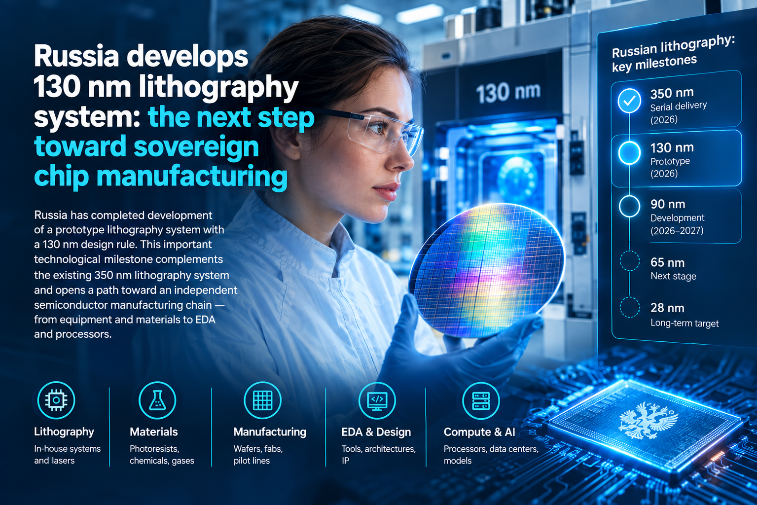
The machine is not yet a production tool. It is a prototype — the end of the third stage of R&D, with an acceptance certificate signed on August 7, 2026. Serial deliveries are planned for 2027. But the significance of the moment is not in the nanometres. It is in what the machine represents: the first serious attempt in decades to rebuild, from the ground up, the ability to manufacture the machines that manufacture chips.
What exactly was built
The system was developed by the Zelenograd Nanotechnology Center (ZNTC) in cooperation with the Belarusian company Planar. It is a projection lithography stepper designed for silicon wafers up to 200 mm in diameter and target feature sizes of 130 nm. Within the project, two prototype excimer lasers operating at 193 nm were manufactured, along with photomasks, test structures, and optical-characterisation equipment.
None of these are trivial achievements. A 193-nanometer excimer laser is the light source that makes deep-ultraviolet lithography possible. Very few countries can design, build, and qualify one. The fact that Russia built its own — rather than importing it — is the part of the story that matters most.
A technological ladder, not a single machine
The 130-nm stepper did not appear from nowhere. It sits on top of a deliberate progression.
The first rung was a 350-nm lithographer. By late 2026, ZNTC was preparing its first serial delivery — the first machine to the company Mapper in December 2026, and the next to a subsidiary of the Element group. The 350-nm machine works with wafers up to 200 mm and is intended primarily for power, automotive, and industrial electronics.
The second rung is the 130-nm stepper now in prototype.
The third rung — 90 nm — is already beyond the idea stage. A technical specification has been prepared, and the selection of contractors is underway.
Beyond that lies 65 nm, and eventually 28 nm. A research and technology centre is nearing completion in Zelenograd that will progressively master topological norms down to the 28-nanometer level.
But the ladder must not be mistaken for a simple scale of resolution. Each step demands more than a new machine. It requires new photoresists, new optical materials, new metrology tools, new chemistry, new EDA software, new process recipes, new engineers — and factories capable of running the process repeatedly, at yield, at scale.
This is why the lithographer is only one element of a much larger system.
The global context is a different game entirely
There is no way to tell this story honestly without acknowledging the distance to the frontier.
While Russia was rebuilding the 130-nm capability, Intel was integrating High-NA EUV into high-volume manufacturing for selected layers of its most advanced processors. ASML and TSMC announced a joint initiative to move toward large-format photomasks for High-NA EUV, with TSMC planning to use the technology for mass production of leading-edge nodes from 2030 onward. More than a million wafers have already passed through High-NA systems for qualification, R&D, and production.
The industry is solving a different problem: how to scale the next generation of computing at 2 nm and below.
Russia is solving a different problem: how to restore and localise the ability to build the equipment that makes microelectronics possible at all.
Comparing the two by nanometres alone misses the point entirely.
It was never only about lithography
Look past the headline and a larger structure becomes visible. In parallel with the lithographer, Russian industry is developing:
- excimer lasers and optical systems;
- photomasks and mask-writing equipment;
- photoresists and chemical materials for 90-nm processes;
- wafer processing, etching, and cleaning equipment;
- ion implantation and inspection tools;
- EDA software;
- silicon wafers and semiconductor substrates;
- production lines;
- domestic processor architectures;
- storage, compute, and data-centre systems.
Over the past three years, roughly sixty critical material and chemical positions have been localised. Another sixty are expected to reach the market by 2029.
This is the part that matters more than any single machine. Because sovereignty in microelectronics cannot be purchased as a product.
Sovereignty is a dependency graph
Picture the production of a modern processor as a chain:
Resources → Materials → Machines → Chips → Compute → Models → Knowledge → Agents → Decisions.
If any single critical link is controlled entirely by an external supplier, the whole system remains dependent.
So technological sovereignty is not the question “do we have our own processor?” The question is much harder: can we maintain, develop, and reproduce the critical technological chain if an external supplier disappears?
The lithographer closes a critical layer in the middle of the stack.
Seen from this angle, the 130-nm lithographer becomes far more interesting than just another machine. It closes a layer of the stack that had been outside the country for a very long time.
Why 130 nm still matters
It is easy to look at 130 nm and say the world moved on decades ago. That is true.
But most of the real economy does not require the most advanced processor on the planet.
Industrial automation. Energy systems. Automotive electronics. Measurement equipment. Specialised controllers. Microcontrollers. Infrastructure hardware. In all of these, mature process nodes remain economically and technically justified.
The goal is therefore not necessarily to produce an immediate domestic equivalent of the most advanced AI accelerator. There is another path: first gain control over a sufficiently mature production loop, then complicate it, then build the next one.
And this is where Sovereign Intelligence begins
The most interesting part of this news is not in microelectronics at all. It is above it.
We talk a great deal today about sovereign AI. But AI cannot be separated from physical infrastructure.
A model requires compute. Compute requires processors. Processors require fabrication. Fabrication requires equipment. Equipment requires materials, optics, lasers, electronics, software, and trained engineers.
The full stack reads:
Resources → Materials → Machines → Chips → Compute → Models → Knowledge → Agents → Intelligence.
That is the wider architecture of Sovereign Intelligence. A lithographer is very far from the model. But without the lower layers, the upper layers cannot be fully controlled.
You do not have to start at 2 nm
Full technological independence is a very long road. Attempting to replicate the entire frontier stack — TSMC plus ASML plus NVIDIA plus Synopsys — at once is effectively an attempt to reproduce an enormous international ecosystem in a single move.
There is another approach: build a sufficiently independent compute loop capable of serving critical workloads.
For some scenarios this does not mean the smallest process node. It means domestic architectures, domestic accelerators, efficient compilation, model optimisation, distributed computing, domestic networking, domestic storage, domestic data centres, efficient cooling, domestic AI infrastructure, domestic data, and domestic orchestration of models and agents.
And then the question changes. Not:
When will we have 2 nm?
But:
Which layers of intelligent infrastructure must we control today?
The real shift happens above the hardware
Sovereign AI does not require a model trained exclusively on domestic chips. It does not even require a fully domestic chip.
It requires the ability to control the critical path:
Compute → Models → Enterprise Knowledge → Agents → Decisions.
Not just computing — but understanding, acting, and deciding within one's own technological environment.
That produces a new architecture. A bottom layer of owned or controlled resources and compute. A middle layer of owned data, models, knowledge, and orchestration. A top layer of agents acting within one's own rules, context, permissions, and infrastructure.
That is no longer merely digital sovereignty. That is Sovereign Intelligence.
What Russia is actually doing
It would be a mistake to overstate the current result. Russia does not yet possess a fully closed production chain for advanced semiconductors. The 130-nm system is at the prototype and acceptance-testing stage. The 350-nm equipment is only entering serial operation. 90 nm is the next development step. The global frontier is at a completely different level, and critical elements of the global semiconductor ecosystem remain unavailable or dependent on external suppliers.
That is precisely why what is happening is interesting.
This is not a story about Russia catching up with the global microelectronics industry. It is a story about something else: the restoration of the ability to create the industrial infrastructure on which microelectronics is built.
If this process continues — from 350 nm to 130, then 90, then 65 and 28, in parallel with materials, EDA, fabs, and processor architectures — the critical dependencies can be progressively reduced.
Sovereignty is a stack, not a chip
Perhaps that is the right way to look at technological independence today.
Not as one national processor. Not as one domestic model. Not as one data centre. Not even as one lithographer.
Sovereignty is the ability to control the technological stack. From physical resources to compute. From compute to models. From models to knowledge. From knowledge to agents. From agents to decisions.
In that sense, the story of the Russian 130-nm lithographer is a small but very concrete fragment of a much larger process.
The world is building the next generation of computing. Russia is simultaneously trying to rebuild the ability to build computing at all.
And it is that second process which may, in the end, prove strategically more important than the race for any single technology node.